

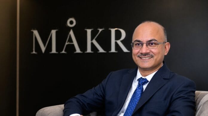
September 4, 2026: Makr Microsystems has secured Rs 10.2 Cr Seed funding. The semiconductor metrology startup will use the capital to advance its subsurface inspection technology, validate it with customers and move towards commercial deployment.
The funding comes as semiconductor manufacturing is becoming increasingly dependent on structures that are difficult to inspect from the surface. Advanced packaging, chiplets and 3D architectures are placing critical interfaces and connections beneath multiple layers of material, making subsurface inspection increasingly important for manufacturers.
Being able to examine these structures can help chipmakers identify defects, understand the quality of interfaces and improve manufacturing yields. However, existing inspection techniques often involve trade-offs between resolution, measurement depth, speed and whether the process damages the chip or sample.
Makr is developing a non-destructive approach aimed at addressing some of these limitations.
Makr Microsystems : A closer look beneath the chip
Its core technology, Acoustic Atomic Force Microscopy (AAFM), combines atomic force microscopy with acoustic sensing to gather information from structures beneath a material’s surface.
The startup is developing the technology into a high-resolution inspection platform for semiconductor applications including advanced packaging, hybrid bonding, buried interfaces, chiplet interconnects and defect detection.
The need for such technology is growing as the semiconductor industry increasingly relies on advanced packaging and three-dimensional integration rather than transistor scaling alone. As more functionality is packed into multiple layers and interconnected components, manufacturers need ways to verify structures that cannot be assessed through conventional surface-level inspection.
“Semiconductor manufacturing is creating structures that are increasingly difficult to see and measure. As architectures move into the third dimension, understanding what is happening beneath the surface becomes critical to improving yield,” said Ashwin Lal, founder of Makr Microsystems.
“Our goal is to make the subsurface measurable, non-destructively and at the resolution the next generation of chipmaking demands.”
Lal holds a Master’s in Physics from IIT Kanpur and a PhD in Microtechnology from EPFL. He previously founded Shilps Sciences and worked as an engineer at Applied Materials.
The immediate focus for Makr is now on taking its technology from development and validation towards commercial use, with customer validation expected to play a key role in that transition.
The Rs 10.2 crore round was led by Bluehill VC, a venture capital fund focused on frontier technology. Artha Venture Fund also participated.
Manu Iyer, General Partner at Bluehill VC, said the firm sees Makr as a company addressing a difficult problem deeper in the semiconductor technology value chain.
“Makr is solving a difficult problem in semiconductor manufacturing at a time when the industry is moving toward increasingly complex architectures. We believe this is a global opportunity, and that world-class semiconductor equipment and technology can be built from India,” Iyer said.

